• PCB Surface Finish Guide: HASL vs. ENIG vs. OSP — How to Pick the Right One

    If you work in hardware, you know the feeling: you’re deep in a PCB design review, and someone asks, “What surface finish are we going with?”

    It sounds like a minor detail. It isn’t.

    Pick the wrong finish, and you’re signing up for yield issues in production, long-term reliability risks in the field, or cost overruns that eat into your margin. Get it right, and nobody notices — which is exactly how it should be.

    The good news is the PCB industry has converged on three dominant surface finish technologies. Each has clear tradeoffs. Know them, and you’ll make the right call every time.

    Let’s break down HASL, ENIG, and OSP — what they are, where they shine, and where they’ll bite you.


    Why Surface Finish Matters in the First Place

    PCB pads are copper. Copper oxidizes when exposed to air. Oxide kills solderability — cold joints, dewetting, high contact resistance. A surprising number of production headaches trace back to this one root cause.

    Surface finish is a thin coating applied to bare copper pads. It does two jobs:

    • Protects the copper from oxidation and corrosion, extending shelf and service life
    • Ensures solderability — so solder wets properly during SMT reflow and through-hole assembly

    Three finishes do most of the heavy lifting in the industry. Let’s go through them one by one.


    1. HASL — The Workhorse

    HASL (Hot Air Solder Leveling) is the oldest and most widely used surface finish in PCB manufacturing. If you’ve been around hardware for more than a few years, you’ve seen thousands of these boards.

    How it works

    The board is dipped into a bath of molten solder, which wets the exposed pads and plated through-holes. As it comes out, hot air knives blow excess solder off the surface and out of the holes, leaving a uniform, shiny tin coating.

    Simple. Proven. Cheap.

    1

    Leaded vs. Lead-Free HASL

    Two variants, and the difference matters:

    • Leaded HASL — tin-lead alloy, lower soldering temperature, better wetting, but contains lead and fails RoHS compliance. Essentially obsolete for new consumer products.
    • Lead-Free HASL (LF-HASL) — lead-free tin alloy (typically Sn-Cu or SAC-based), RoHS compliant, runs at higher temperatures, slightly higher risk of dewetting if process parameters aren’t tight.

    What’s good about HASL

    • Proven solderability — decades of real-world use. Solder wets well, and the process is well understood by every fab house on the planet.
    • Good electrical conductivity — solid performance for most applications.
    • Low cost — the most economical mature finish available.

    Where HASL falls short

    • Poor surface flatness — this is the big one. Molten solder + surface tension + gravity = a “pillowing” or “turtle-back” effect where pads are slightly domed in the center. Fine-pitch components hate this.
    • Not for fine-pitch or BGA — the uneven surface makes HASL a poor fit for high-density SMT with small packages or tight pitch.
    • Lead-free HASL runs hotter and can be trickier to dial in.

    Best for

    General-purpose, cost-sensitive boards with larger component pitch. If your design is through-hole or large SMD components and cost is the driving factor, HASL is the default.


    2. ENIG — The Premium Choice

    ENIG (Electroless Nickel Immersion Gold) is the go-to finish when flatness, reliability, and shelf life matter most.

    As electronics have trended toward miniaturization, higher density, and tighter reliability requirements, HASL’s limitations became impossible to ignore. ENIG stepped in to fill the gap.

    How it works

    ENIG is a two-layer metallic coating deposited chemically — no electrical current required:

    1. A nickel layer is first deposited by autocatalytic chemical reaction. This is the structural layer and the diffusion barrier.
    2. A thin gold layer is deposited on top via immersion plating. It protects the nickel from oxidation and provides a highly solderable surface.

    The result is an extremely flat pad surface — ideal for fine-pitch and high-density assembly.

    BGA

    If you’ve ever looked at a BGA pad array under a microscope, you’ve seen ENIG at its best. Every pad is uniformly gold and mirror-flat. For BGA packages, where coplanarity of every solder ball is make-or-break, HASL’s “turtle-back” effect would cause immediate reliability failures. ENIG eliminates that problem entirely.

    What’s good about ENIG

    • Exceptional flatness — smooth, uniform pad surfaces that are perfect for high-density SMT and fine-pitch components.
    • Excellent solderability — compatible with SMT, through-hole, and pretty much any assembly process you throw at it.
    • Superb stability — the dense gold crystal structure gives you excellent oxidation resistance, wear resistance, and corrosion resistance. Shelf life is long.
    • Wear resistance — gold is hard. That matters for gold fingers, keypads, and any sliding or mating contact.
    • Lead-free and RoHS compliant.

    Where ENIG falls short

    • Cost — significantly more expensive than HASL or OSP. Gold isn’t cheap, and neither is the process.
    • Process complexity — more chemical steps, longer processing time, more things that can go wrong if the fab isn’t careful. Black pad is a known failure mode if the process isn’t controlled.

    Best for

    • BGA packages, fine-pitch QFP, and any component where pad flatness is critical
    • High-frequency / high-speed boards where signal integrity matters
    • Gold fingers, keypads, and connectors — anywhere wear resistance and stable contact resistance are required
    • Products with long shelf life requirements

    Rule of thumb: if your design includes BGA or fine-pitch QFP, default to ENIG. The cost premium is worth the reliability peace of mind.


    3. OSP — The Budget Performer

    OSP (Organic Solderability Preservatives) is an organic coating that protects copper from oxidation while maintaining excellent solderability.

    It’s the cheapest finish available, and when used in the right application, it punches well above its weight class.

    How it works

    A thin organic film is chemically deposited onto the clean copper surface. This film prevents oxidation during storage and handling, but dissolves completely and quickly when exposed to flux during soldering — exposing fresh copper that bonds directly with the solder.

    Early organic coatings were rosin-based, but rosin had real problems: it absorbed moisture, got sticky, and could oxidize and harden on the board over time. Modern OSP formulations have largely replaced it.

    Because the film is so thin, OSP pads look almost like bare copper — and they’re perfectly flat. The coating doesn’t change pad geometry at all.

    OSP

    What’s good about OSP

    • Excellent flatness — the organic film is ultra-thin, so pad geometry is essentially unchanged. As flat as the copper underneath.
    • Environmentally friendly — lead-free, RoHS compliant.
    • Good solderability — compatible with SMT, through-hole, and most common assembly methods.
    • Lowest cost — the most economical surface finish option available.

    Where OSP falls short

    • Heat sensitivity — OSP can degrade or break down after multiple high-temperature soldering cycles. Multiple reflow passes are a problem.
    • Short shelf life — storage time is limited compared to metallic finishes. Performance degrades over time, and oxidation risk increases with age. Use it or lose it.

    Best for

    • Simple, low-cost boards with straightforward assembly
    • Single- or double-sided boards with uncomplicated designs
    • Thermal separation copper substrates — simple structure, mostly large power devices, and cost is a key driver
    热电分离

    For example, thermal separation copper substrates used in high-power LED applications: the heat path goes directly through the copper base, assembly is dominated by large power devices, and the structure is simple. OSP delivers excellent flatness and solderability at minimal cost.


    Quick Comparison

    Here’s how the three finishes stack up across the key dimensions: Leaded HASL Lead-Free HASL ENIG OSP Flatness Poor Fair Excellent Excellent Solderability Good Good Excellent Good Oxidation resistance Fair Fair Excellent Fair Wear resistance Fair Fair Excellent Poor Cost Low Medium High Lowest RoHS compliant No Yes Yes Yes Fine-pitch / BGA No No Yes Yes Shelf life Long Long Long Short Multiple reflows Good Good Excellent Poor


    5 Rules for Choosing the Right Finish

    1. Consumer electronics, cost-sensitive, large-pitch components → Lead-free HASL. Leaded is essentially dead for new consumer products due to RoHS.
    2. BGA / fine-pitch QFP / high-speed boards → ENIG. Flatness and reliability aren’t optional here.
    3. Simple boards, low cost, fast inventory turnover → OSP. Best value by far, but watch the shelf life — don’t let boards sit in a warehouse for six months.
    4. Gold fingers / keypads / sliding contacts → ENIG. Wear resistance and stable contact resistance are the whole game.
    5. Aluminum substrates / thermal separation copper substrates → OSP for simple structures; ENIG if high reliability is required.

    The Bottom Line

    There is no “best” PCB surface finish. There’s only the best fit for your constraints.

    The decision always comes down to balancing four factors: flatness, solderability, reliability, and cost.

    • Maximum flatness and reliability → ENIG
    • Maximum cost efficiency → OSP
    • Balanced performance and proven maturity → HASL

    Before you lock in a choice, list your hard constraints first: BGA pitch, operating environment, shelf-life requirements, and cost target. Work through the tradeoffs against those constraints, and you’ll usually narrow it down in two or three passes.


    What’s your go-to surface finish? And have you ever had a finish-related failure in production that taught you a hard lesson? Drop a comment — I’d love to hear your war stories.


    If you found this useful, subscribe to my newsletter for more deep dives on LED products management,technique,marketing and the smart lighting industry.
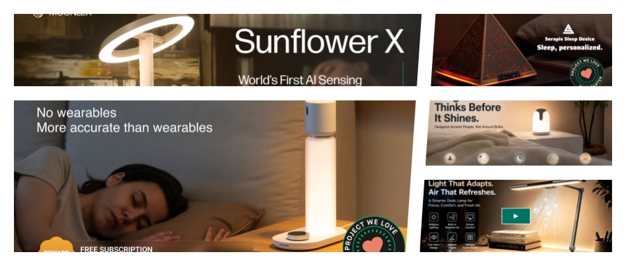
  • A Product Manager’s Deep Dive into 5 Sleep Lamps: Each One Is Redefining What a “Lamp” Can Be

    💡 Ever wondered what happens when you cross the most traditional hardware category with AI, sensors, and a dose of startup creativity?

    I recently dived into Kickstarter to find out—not as a shopper, but as a product manager who’s spent 15 years in the lighting industry. What I discovered surprised even me.

    Just in the “sleep + smart lighting” niche alone, there are over a dozen products with wildly different approaches. Each one is answering the same question: when illumination is no longer a scarce resource, what else can a lamp do?

    Below is a breakdown of five standout products using a three-part framework: Use Case → User Value → Key Features. I’ll wrap up with my overall takeaways at the end.


    1. Sleepal AI Lamp — Bringing the Sleep Lab to Your Nightstand

    image

    In a word: The world’s first non-contact bedside AI sleep system, using mmWave radar + multi-sensor fusion to create a bedside lamp that actually improves your sleep.

    Use cases: Pre-sleep relaxation, in-sleep monitoring with environment sync, night-time motion-activated lighting, and gentle wake-up during light sleep cycles.

    User value: The biggest value is effortlessness—no wristband, no electrodes, no setup. Just lie down and it starts working. And it doesn’t just give you a sleep score: it correlates snoring with sleep position, analyzes environmental factors, and delivers actionable advice from an AI coach. These are features that genuinely help you sleep better.

    Key features:

    • Six-sensor fusion: mmWave radar + sound + thermal + ambient light + temperature & humidity
    • Clinical-grade AI: Trained on hospital PSG data, with respiratory rate accuracy on par with medical devices
    • Privacy-first: Pure physical sensing, on-device processing, your data is never used to train models
    • Freemium model: Basic features free; AI sleep staging and coaching via subscription

    2. Sunflower X — The Sunflower-Shaped AI Sunrise Alarm Lamp

    image

    In a word: A 60GHz mmWave radar + auto-rotating light ring that takes “natural wake-up” to the extreme.

    Use cases: Gentle wake-up during light sleep windows, gradual dimming for falling asleep, motion-activated night light, and everyday reading/ambient lighting.

    User value: It solves a very specific pain point: the misery of waking up. Traditional alarms jolt you awake—this one waits until your body is ready. Using progressive light and sound stimulation, you wake up with significantly less grogginess.

    Key features:

    • Auto-rotating light ring: Sunflower design—light spreads from a point to full coverage like a sunrise, instantly recognizable
    • 60GHz radar: 7 scans per second, 240,000+ data points per night, detecting chest wall displacement down to 0.1mm
    • SureWake dual-layer wake-up: Light first, then sound—gradually intensifying to ensure you wake up without being startled
    • AI sleep coach: Doesn’t just give you data—it explains why and offers lifestyle recommendations

    3. Serapis — 5-in-1 All-Scenario Sleep Aid Device

    image

    In a word:: Schumann resonance + white noise + breathing light + fractal visuals + pyramid acoustics—all in one app-free, minimalist device.

    Use cases: Racing-thought insomnia (fractal visual guidance), environment-sensitive insomnia (white noise masking), and jet lag/schedule disruption (light-sound rhythm sync).

    User value: The biggest value is simplicity—no app, no account, no Bluetooth pairing. Unbox it, put it on your nightstand, press a button, and you’re done. With five sensory inputs working simultaneously, it has a higher success rate for people who’ve “tried everything and nothing works.”

    Key features:

    • Five-mode synergy: Schumann waves + layered white noise + breathing light + fractal visuals + pyramid acoustics
    • Sleep type assessment first: Helps you identify “what kind of insomnia you have” before recommending a mode—educating users while improving conversion
    • Zero digital friction: No app, no subscription, no data upload
    • Strong scientific narrative: Every feature is backed by a framework of scientific discourse, making users feel “this isn’t pseudoscience”

    4. Elunvia — The Smart Lamp That “Looks Away From Your Eyes”

    image

    In a word:: A 24GHz radar tracks your position and automatically redirects light to the wall behind you for 100% glare-free illumination.

    Use cases: Glare prevention for screen workers, reflection-free night reading, motion-activated night light for couples sharing a bedroom, zero-blue-light gradual dimming before bed, and sunrise simulation in the morning.

    User value: It solves a problem you might not realize you have but is always there—most lamps shine directly at you, and glare + reflected light are quietly wearing down your eyes. Elunvia’s logic is counterintuitive: a good lamp shouldn’t let you see the light source.

    Key features:

    • Radar tracking + auto-rotation: Detects where you are, swivels the lamp head away, and bounces light off the wall. The tech isn’t hard—the product insight is spot-on
    • Truly zero-blue-light LED: Not “low blue light” and not a filter—blue light is eliminated at the chip level
    • 7 scenarios in one: Bedside / reading / desk / whole-room / night light / wake-up / ambient
    • Four control methods: Touch / App / NFC / timer—an entry point for every user preference

    5. LUMORA — The Desk Lamp That Brings “Forest Air” to Your Workspace

    image

    In a word:: Dual-layer optical system + negative ion air system, creating a “forest-like” desktop light environment.

    Use cases: Long hours of work or study, screen-based work, focused reading, pre-sleep relaxation, and when indoor air quality is poor.

    User value: It’s not selling “a brighter lamp”—it’s selling a more comfortable desktop environment. By combining light and air, and packaging it as “forest feeling,” it delivers both functional benefits and emotional resonance.

    Key features:

    • Dual-layer optics: Forward task light + rear ambient light, reducing contrast between bright and dark
    • Integrated negative ion system: Low cost, but elevates the product positioning from “desk lamp” to “desktop environment system”
    • EML circadian lighting: Automatically adjusts the melatonin-affecting spectrum throughout the day
    • Four modes for four scenarios: Reading & Focus / Screen Comfort / Relax & Sleep / Daily Rhythm

    Three Observations From a Product Manager

    After breaking down these five products, three strong impressions stand out:

    First, the “lamp” category is being redefined.

    Metrics that used to be the core—luminous efficacy, color rendering index, lifespan—are becoming table stakes. The new competitive dimension is: can this lamp sense me, understand me, adapt to me, and help me become better?

    Second, both “less is more” and “more is everything” strategies are valid.

    Banala and Serapis go minimalist—no app, no data, one-button operation. Sleepal and Sunflower X go all-in—radar + AI + IoT + subscription, maxed-out features. Neither is right or wrong—the key is which type of user you’re targeting.

    Third, great products all have a one-liner memory hook.

    Sunflower X is “the rotating sunflower lamp.” Elunvia is “the lamp that looks away from your eyes. If your product takes three sentences to explain, users probably won’t remember it.

    Anyone in product knows: the hardest part isn’t adding features—it’s finding that one reason why people must choose you.


    🤔 Your turn: Which of these five approaches resonates most with you? Are you a “minimalist, one-button” person, or do you prefer the full-stack sensor + AI experience?

    I’d love to hear your thoughts—drop a comment below.

    #SmartLighting #ProductManagement #SleepTech #IoT #HardwareStartups #ConsumerElectronics #AI #Innovation #ProductDesign

  • Why PLC Mesh Is Indispensable for Smart Home Networking in China

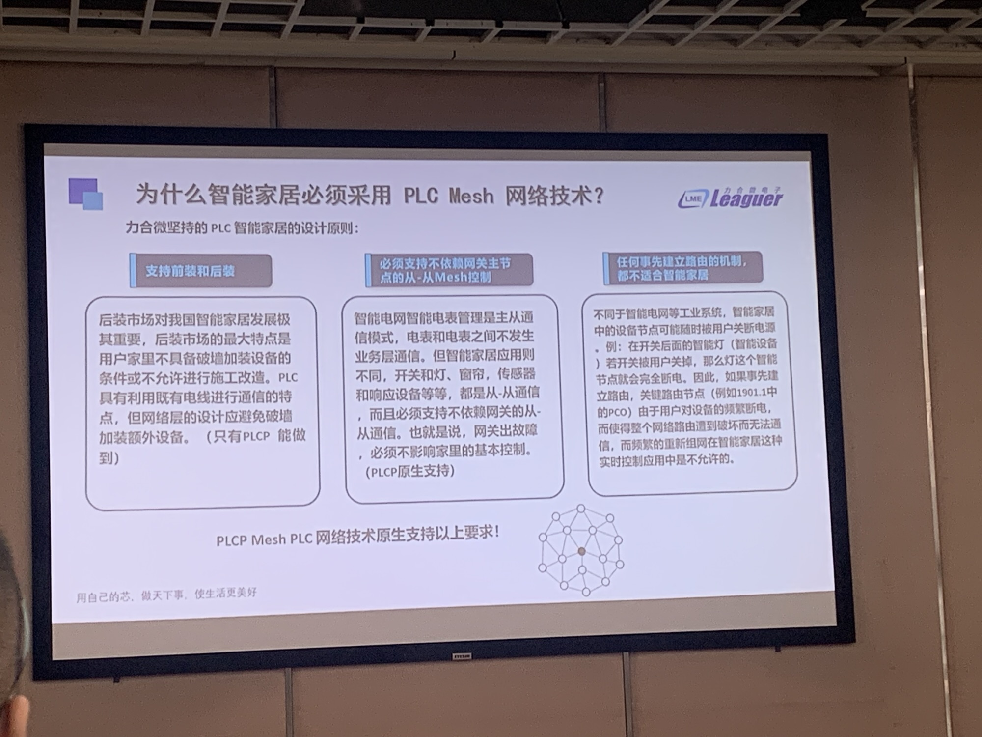
    Technical design principles behind Leaguer’s PLC-based smart home architecture.


    Principle 1: Native Support for Both Pre-construction and Retrofit Deployment

    The retrofit market represents a critical growth vector for smart home adoption in China. Its defining constraint is that existing residential premises lack the structural provisions for in-wall equipment installation, and occupants typically will not tolerate invasive renovation work.

    PLC technology leverages the existing power line infrastructure as a physical transmission medium. Crucially, however, the network layer architecture must be designed to operate without requiring additional hardware to be installed behind walls.

    This capability is unique to PLCP.


    Principle 2: Decentralized Slave-to-Slave Mesh Operation — No Gateway Dependency

    Conventional smart grid architectures employ a master-slave communication paradigm, in which field devices (e.g., smart meters) exchange data exclusively with a central controller and never peer with one another at the application layer.

    Smart home environments operate under fundamentally different constraints. Switches, luminaires, motorized curtains, sensors, and actuators must all communicate directly in a peer-to-peer fashion, independent of any central gateway.

    The operative requirement: a gateway failure must never compromise basic device control within the home.

    PLCP provides native support for this topology.


    Principle 3: Pre-computed Routing Is Fundamentally Incompatible with Smart Home Dynamics

    Unlike industrial systems and smart grids — where nodes are continuously powered and network topology is stable — smart home deployments face an inherent challenge: end-users can and do cut power to individual device nodes at any time.

    Illustrative scenario: A smart luminaire installed downstream of a wall switch. When the user toggles the switch off, that node loses power completely. If the network relies on pre-computed routing tables, the removal of a critical routing node (such as the PCO specified in IEEE 1901.1) can fracture the entire network topology, rendering communication paths unavailable.

    Frequent re-networking events induced by such intermittent power states are unacceptable for real-time control applications in the smart home context.


    Conclusion

    PLCP Mesh PLC networking technology natively satisfies all three architectural requirements outlined above.

  • China’s “Lighting Capital” Under Scrutiny: CCC Certification Fraud Exposed in Zhongshan

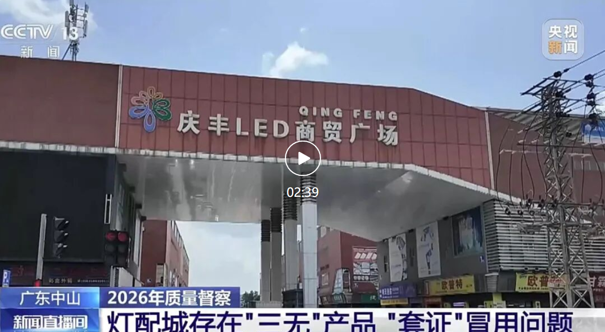
    A recent national quality inspection in Zhongshan, Guangdong — China’s lighting manufacturing hub that accounts for over 60% of domestic civilian lighting sales — has revealed widespread quality and certification violations.

    Key findings from the undercover investigation:

    🔹 Fake CCC labels on “three-no” products: Many LED fixtures displayed CCC marks but lacked manufacturer names, addresses, and valid certification documents.

    🔹 “Universal certificates”: Some retailers openly admitted that one CCC certificate was being reused across multiple product models and power ratings (20W to 70W) — a practice known as “certificate borrowing.”

    🔹 Fictitious company names: One batch of 11 cases of LED panel lights bore the name of a company that doesn’t exist in the national business registry.

    🔹 Production despite revoked certification: One manufacturer (Guangdong Yixun Lighting) continued assembling fixtures even after its CCC certificate was revoked. 18 out of 19 sampled batches (1,430 units) failed quality tests.

    Why this matters: Lighting products connect directly to 220V mains. China’s mandatory CCC certification exists specifically to protect consumer safety. When manufacturers hide their identity and forge certifications, they deliberately break the traceability chain — making it impossible to hold anyone accountable when failures occur.

    Zhongshan authorities have launched investigations into all implicated parties and initiated a city-wide quality improvement campaign for the lighting industry.

    For global buyers sourcing from China’s lighting supply chain, this is a timely reminder: CCC markings alone are not enough. Supplier verification, factory audits, and independent testing remain essential guardrails.

    (For more details,please visit the below Chinese contents link https://mp.weixin.qq.com/s/ot8HL7vIh2_dgBxDfCxrrA )

    #LightingIndustry #QualityControl #CCCCertification #SupplyChain #ChinaManufacturing #ProductSafety #LEDLighting

  • Govee at IFA 2026: AI Lighting Bot 2.0, Sky Ceiling Light, and the Permanent Outdoor Lights 2 Pro — A Product Manager’s Deep Dive

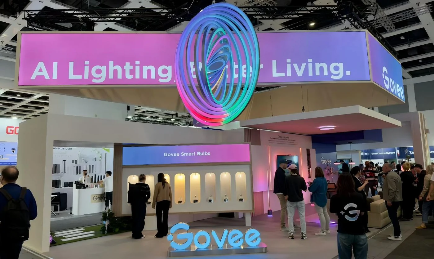
    If you follow smart lighting, this past week felt like a turning point. IFA Berlin 2026 opened its doors on September 4, and Govee didn’t just show up — it dropped four flagship products in three days, broke a 57-day PR silence, and staked its claim that AI is no longer a marketing buzzword for lights.

    As a product manager watching from the industry side, I’ve been tracking Govee’s roadmap closely. This week’s announcements are worth unpacking because they signal where the entire smart lighting category is heading: AI-native control, health-focused spectrum, and Matter as table stakes.

    The IFA 2026 Product Drop: Four Flagships in One Week

    Govee’s booth in Hall 1.2, Stand 124 was built around the theme “Light That Reads the Room.” Here’s what actually launched:

    Govee Sky Ceiling Light (21″) — $399.99 / €399 The headline product. Marketed as the industry’s first AI mood-sensing ceiling light, it packs a custom 478nm sky-blue wavelength (branded “Vitality Spectrum Technology”), 7000 lumens of white light, CRI 95, TÜV Rheinland certification for flicker-free and low-glare, and RG0 blue-light safety. It also supports DaySync circadian rhythm adjustment and Matter out of the box — no Govee Hub required.

    What stands out to me is the edge-lit design. This isn’t a flat panel; it’s engineered to simulate “natural light through an opening,” which is a deliberate move upmarket from basic RGB ceiling fixtures. Govee is clearly building a full “light and health” tech stack: 478nm spectrum + RG0 safety + TÜV certification + DaySync. Competitors with health-focused positioning now have a concrete benchmark to match.

    Govee COB Strip Light 2 Pro (5m) — $169.99 / €179.99 The second-generation flagship strip raises the density bar: 1344 LEDs/m with 16 ICs per meter, a three-layer recessed design, RGBWWIC color mode, and LuminBlend+ color management. Color temperature spans 1000K–10000K with CRI 92. It’s also one of the first products shipping with AI Lighting Bot 2.0 built in.

    Govee COB Strip Light 2 (5m) — $99.99 / €119.99 The base model sits at a more accessible price point with “Next-Gen COB” and RGBIC technology. Notably, Govee hasn’t published full specs for the standard version yet — LED count, IC density, CRI, and color temperature range are all unconfirmed on the product page. That’s an unusual gap for a launch, and worth watching.

    Govee Permanent Outdoor Lights 2 Pro

    Govee Permanent Outdoor Lights 2 Pro — 499.99(100ft)/499.99(100ft)/799.99 (200ft) This one is the most technically interesting. Govee is claiming an industry first: a dual-layer independent IC design (branded “ColorZone Solution”) where each light head has two separate IC chips controlling upper and lower light zones independently. A single fixture can display two different colors or effects simultaneously, with a tilted base design to project them in different directions.

    Add IP68 waterproofing, LuminBlend+ color management, 1000K–10000K range, eight “Iconic Wonders” preset scenes, Y-splitter cables for flexible routing, and Matter support — and you’ve got Govee’s most ambitious outdoor product yet. Brightness stays at 55 lumens per bulb, roughly the same as the previous generation, so the upgrade story is entirely about color capability, not raw output.

    AI Lighting Bot 2.0: From Gimmick to Infrastructure

    Govee CEO Eric Wu’s IFA keynote set the tone clearly: “AI is no longer a marketing gimmick for lighting — it’s the underlying infrastructure that makes lighting more adaptive and responsive to human emotions and daily needs.”

    That’s a bold framing. Here’s what AI Lighting Bot 2.0 actually delivers:

    • Multimodal input: Generate lighting scenes from text, voice, or image
    • Multi-turn conversation: The first lighting AI that supports iterative refinement — you can tweak a scene in dialogue instead of starting over each time
    • Full-scene coverage: AI capabilities expanding from indoor-only to include outdoor products in 2026
    • Group control (roadmap): AI-driven multi-device synchronized group control was announced but not dated

    There’s one notable gap: Govee hasn’t disclosed whether AI processing happens locally, in the cloud, or hybrid. A few outlets (including wpnews.pro) have flagged this as a transparency issue, especially for users concerned about privacy and latency.

    For product managers in this space, the multi-turn conversation feature is the most strategically significant. If it works well, it fundamentally changes how users interact with smart lighting — from picking presets in an app to describing what they want conversationally. The bar for “good smart lighting UX” just got higher.

    The Bigger Picture: PR Silence, IPO Rumors, and Competitive Pressure

    This IFA drop was preceded by a 57-day PR blackout — from July 6 to September 3, Govee issued zero press releases. Then on September 3, a single PR Newswire blast dropped everything: four new products, the AI 2.0 strategy, CEO quotes, and full pricing. That’s a textbook “concentrated fire” launch playbook, and it’s consistent with Govee’s established rhythm of big reveals at IFA and CES.

    A few other signals are worth noting:

    • Patent portfolio growth: Govee’s parent company, Shenzhen Zhiyan Technology, now lists 1,080+ core patents on its official site — up from 870 previously, a 24% jump. That’s the kind of acceleration you see ahead of an IPO.
    • Aqara entering the ring: AOL reported this week that Aqara’s new smart lighting line is “coming for Govee and Philips Hue.” More competition at the mid-to-premium tier is coming.
    • Light Festival 2026 wrapped: Govee’s user-generated content contest across seven platforms (Instagram, TikTok, Facebook, X, Threads, Bluesky, and the Govee Home Community) announced 35 winners on September 7. The contest also served as a quiet pricing test — four unreleased products had their prices first disclosed in contest terms and conditions, then confirmed at IFA.

    What This Means for the Smart Lighting Industry

    Let me distill this down to the three shifts that matter most if you build, sell, or buy smart lighting:

    1. AI is moving from “feature” to “control paradigm.” Govee isn’t the first to put AI in a lighting app, but it’s the first major brand to position AI as the primary interface — and to back it up with multi-turn conversation. Competitors whose app UX is still “tap a preset, slide a slider” need a plan.
    2. Health and wellness is the new premium battleground. The Sky Ceiling Light’s full health stack — 478nm spectrum, circadian sync, TÜV certification, RG0 safety — is the most complete offering we’ve seen from a consumer brand at this price point. Philips Hue has owned “premium quality,” but Govee is redefining what premium means.
    3. Matter is no longer a differentiator — it’s expected. Every flagship Govee announced at IFA supports Matter. If your 2026/2027 product roadmap doesn’t have Matter as a baseline, you’re already behind.

    Govee didn’t just launch new products at IFA 2026 — it set the agenda for the next 12 months of smart lighting. The question for everyone else in the category is whether they can keep up, or whether they’ll find a different lane entirely.

    All product names, trademarks, and prices referenced are property of Govee Moments Limited. Pricing and availability based on US and EU listings as of September 7, 2026.

  • FPCB Manufacturing Process: Step-by-Step Guide (2026)

    Have you ever held a flexible LED strip and wondered how such a thin, delicate piece of film can carry current, resist bending, and survive soldering temperatures? The answer is a surprisingly complex manufacturing process that transforms raw copper-clad film into precision flexible circuits.

    Understanding the FPCB manufacturing process isn’t just factory trivia — it helps you design better products, troubleshoot quality issues, and communicate more effectively with your FPCB suppliers.

    Let’s walk through the process step by step.


    Step 1: Cutting (Sheeting)

    The process starts with raw material in roll form — typically copper-clad PI film (copper foil bonded to polyimide film with adhesive).

    What happens:

    • The roll of raw material is cut into individual sheets of the required size
    • Large sheets may be further cut into smaller panels to maximize material utilization
    • The size is determined by the manufacturer’s equipment and the panel layout efficiency

    Why it matters: Panel layout directly affects your unit cost. Better nesting = more pieces per panel = lower cost per unit. This is why odd-shaped FPCBs can be more expensive — they waste more material.


    Step 2: Drilling

    Next, holes are drilled through the panel. These serve two purposes:

    • Tooling/registration holes — used to align layers and fixturing throughout the process
    • Component holes / via holes — for through-hole components or for connecting top and bottom copper layers (on double-sided FPCBs)

    Two drilling methods:

    MethodHow It WorksBest For
    Mechanical drillingPhysical drill bit spins and cutsLarger holes, thicker materials, lower cost for standard holes
    Laser drillingLaser beam ablates the materialVery small holes (microvias), fine-pitch designs, thinner materials

    For double-sided FPCBs, this step is critical — the vias are what allow electrical connection between the top and bottom copper layers.


    Step 3: Copper Plating (PTH — Plated Through-Hole)

    After drilling, the holes are just bare holes through the film. They need a conductive copper coating to connect the layers.

    This happens in two stages:

    Electroless Copper (PTH / Desmear + Electroless)

    • First, the hole walls are cleaned and etched to create a rough surface for adhesion
    • Then a thin layer of copper (typically 1–2 µm) is chemically deposited on all surfaces — including the hole walls — using an electroless (no external current) chemical reaction
    • This creates a continuous conductive path from top copper to bottom copper

    Electroplating

    • The panel goes into an electroplating bath where additional copper is deposited using electric current
    • This builds up the copper thickness on the surface and in the holes to the required specification
    • Typical plating adds 20–30 µm of copper, depending on the design requirements

    The purpose: Make the through-holes electrically conductive so the top and bottom copper layers are connected. This is the foundation of any double-sided or multilayer FPCB.


    Step 4: Dry Film Lamination

    Now we’re ready to create the circuit pattern. First, a photosensitive dry film is applied to both sides of the copper-clad panel.

    What happens:

    • The dry film (a photoresist material) is laminated onto the copper surface under heat and pressure
    • The film adheres tightly to the copper
    • It will act as a photographic mask — after exposure and development, it protects the copper we want to keep during etching

    This is the first step in the photoimaging process — essentially using light to “print” the circuit pattern onto the board.


    Step 5: Exposure

    The circuit pattern is transferred from the design file to the dry film using photographic exposure.

    What happens:

    • A phototool (film artwork) is created from the Gerber design files — it’s essentially a photographic negative of the circuit pattern
    • The phototool is aligned with the panel (using those registration holes drilled in Step 2)
    • UV light shines through the phototool onto the dry film
    • Areas of the dry film exposed to UV light polymerize (harden) — these become resistant to the developer chemical
    • Areas not exposed to light remain soluble

    Think of it like developing film in a camera — except the “picture” is your circuit layout, and the “film” is a thin plastic layer on copper.


    Step 6: Developing

    After exposure, the panel goes through a developer solution (usually sodium carbonate or potassium carbonate).

    What happens:

    • The unexposed (unpolymerized) dry film is washed away
    • The exposed (hardened) dry film stays in place, protecting the copper underneath
    • What you’re left with is copper covered by a dry-film “stencil” that exactly matches your circuit pattern — the copper that will become your traces is protected, and the copper you want to remove is exposed

    At this point, you can actually see the circuit pattern forming on the panel.


    Step 7: Etching

    This is where the real magic happens — the unwanted copper is removed, leaving only the circuit traces.

    What happens:

    • The panel is sprayed with etching solution (typically ferric chloride or an alkaline etchant) at a controlled temperature
    • The etchant chemically reacts with the exposed copper (the copper not protected by dry film) and dissolves it away
    • The copper under the hardened dry film is protected and remains
    • The result is the actual copper traces of your circuit

    Etching is one of the most critical process steps — too much etching and your traces become thinner than designed (affecting current capacity and impedance); too little and you get shorts between traces.


    Step 8: Stripping (Dry Film Removal)

    After etching, the dry film has done its job and needs to be removed.

    What happens:

    • The panel is treated with a strong alkaline solution
    • The hardened dry film is dissolved and stripped away
    • What’s left is the bare copper circuit pattern on the flexible substrate — your FPCB traces, fully formed and visible

    At this stage, the basic circuit is complete. But we’re not done yet — we still need to protect it, add surface finishes, and test it.


    Step 9: Coverlay Lamination (Layup + Pressing)

    For FPCBs, the equivalent of solder mask on rigid PCBs is usually a coverlay (cover film) — a layer of PI film with adhesive, laminated over the circuit traces.

    Two sub-steps:

    Layup (False Bonding)

    • The coverlay film (PI + adhesive, with openings cut for pads) is carefully positioned over the panel
    • It’s temporarily tacked in place with light heat and pressure

    Lamination / Pressing

    • The panel with coverlay goes into a hot press (vacuum lamination press)
    • Under high temperature and pressure, the adhesive flows and the coverlay is permanently bonded to the circuit
    • The result is a protective dielectric layer over all the copper traces, with only the pads exposed

    Why coverlay instead of solder mask? Coverlay is much more flexible and resistant to bending fatigue — critical for FPCBs that will be flexed. Solder mask ink can crack when bent, which is why true flexible circuits use coverlay.


    Step 10: Solder Mask Printing & Silkscreen

    In addition to (or instead of) coverlay, some FPCBs have solder mask and silkscreen printed on them:

    • Solder mask — a liquid ink (often white for LED applications) printed and cured to protect copper and prevent solder bridges. For LED strips, white solder mask under the LEDs improves light reflectivity.
    • Silkscreen / Legend printing — text, logos, part numbers, polarity marks, and other markings printed onto the board for identification and assembly guidance

    This step uses screen printing or inkjet printing technology, and the ink is cured with UV light or heat.


    Step 11: Surface Finish

    The exposed copper pads need a protective coating to prevent oxidation and ensure good solderability. This is the surface finish step.

    Common surface finishes for FPCBs:

    • OSP (Organic Solderability Preservative) — thin organic coating, low cost, flat surface. Most common for LED strips.
    • ENIG (Electroless Nickel Immersion Gold) — nickel + gold, excellent solderability, supports wire bonding. Higher cost.
    • Electrolytic Gold Plating — for edge connectors / gold fingers.
    • Tin Plating — for solderability or etch resist.
    • HASL (Hot Air Solder Leveling) — less common on FPCBs due to high temperature.

    The surface finish is applied only to the exposed copper pads — not to the areas covered by coverlay or solder mask.


    Step 12: Final Inspection & Shipping

    Before the FPCBs leave the factory, they go through quality control:

    • FQC (Final Quality Control) — visual inspection, dimensional check, electrical test (continuity / insulation resistance), AOI (Automated Optical Inspection)
    • Sampling inspection — statistical sampling to verify overall quality
    • Packaging — FPCBs are carefully packaged (often on reels or in trays) to prevent damage during shipping
    • Shipping — delivered to the customer or sent to the SMT assembly house

    The Full Process at a Glance

    1. Cutting — raw roll material cut to panel size
    2. Drilling — tooling holes and via holes
    3. Copper plating — PTH + electroplating to make holes conductive
    4. Dry film lamination — photosensitive film applied to copper
    5. Exposure — UV light transfers circuit pattern from phototool to dry film
    6. Developing — unexposed film washed away, revealing the pattern
    7. Etching — unwanted copper dissolved, leaving circuit traces
    8. Stripping — dry film removed, exposing bare copper circuits
    9. Coverlay lamination — protective film laminated over circuits
    10. Solder mask & silkscreen — printing and marking
    11. Surface finish — pad protection (OSP, ENIG, etc.)
    12. Inspection & shipping — QC, packaging, delivery

    Why This Matters for Your LED Products

    Understanding the manufacturing process helps you:

    • Design for manufacturability (DFM) — know what’s easy vs. expensive to produce
    • Troubleshoot quality issues — if you see trace undercutting, you know it’s an etching problem; if vias fail, it’s likely a plating issue
    • Negotiate with suppliers — speak the same language as your FPCB vendor
    • Estimate lead times — know which steps add time and cost

    In the next and final article of this series, we’ll look at the key performance parameters of FPCBs — including voltage drop — and how to calculate the right trace width and copper thickness for your LED design.

    Version 1.0,Content by LED Product Manager,Time Sept-10-2026,Space Dongguang

  • FPCB Materials and Layer Structure: A Complete Guide for LED Engineers

    Flexible Printed Circuit Boards (FPCBs, or FPCs) are everywhere in modern LED products — from flexible LED strips and COB strips to wearable lights and curved display backlights. But if you’ve ever wondered why some FPCBs crack after a few bends while others last thousands of cycles, the answer lies in the materials and layer structure.

    Let’s break down what FPCBs are made of, how they’re built, and what each layer contributes to performance.

    What Is an FPCB?

    FPCB stands for Flexible Printed Circuit Board (often shortened to FPC). It’s a printed circuit board built on a flexible base material — typically polyimide (PI) or polyester (PET) film — instead of rigid fiberglass.

    Key advantages over rigid PCBs:

    • Flexibility — can be bent, folded, wrapped, or dynamically flexed
    • Thin & lightweight — saves space and weight in compact designs
    • High wiring density — more connections in less area
    • Automated production — consistent quality, fewer wiring errors
    • 3D packaging — fits into curved or irregular enclosures

    For LED products, this means you can create strip lights that wrap around furniture, thin backlight panels for displays, and wearable light designs that conform to the body.


    Core Materials of FPCB

    An FPCB is a sandwich of several material layers. Let’s look at each one.

    1. Conductive Layer — Copper

    The copper layer carries the electrical current. Two main types of copper foil are used in FPCBs:

    PropertyRolled Annealed Copper (RA Copper)Electrodeposited Copper (ED Copper)
    ManufacturingRolled and annealed multiple timesElectroplated from electrolyte solution
    Crystal structureFlaky/lamellar, fine grains, orderedColumnar, larger grains, less ordered
    Purity~99.9%99.95%+
    Flex enduranceExcellent — better for dynamic flexFair — better for static flex
    Ductility / elongationLowerHigher
    Best forDynamic flex applications, hinge areasStatic applications, fine-pitch traces

    Rule of thumb: If your LED strip will be bent or folded repeatedly (e.g., a strip installed around corners and edges), RA copper is the better choice. For static installations where the FPCB is bent once during assembly and then stays in place, ED copper works fine and is usually cheaper.

    2. Insulating Substrate — Base Film

    The base film provides mechanical support and electrical insulation. Two common materials:

    • PI Film (Polyimide Film) — The industry standard for high-performance FPCBs.
      • Excellent thermal resistance (can handle soldering temperatures)
      • Good moisture resistance
      • Strong peel strength (copper adheres well)
      • Yellowish/amber appearance
      • Use case: Most LED strips, automotive, industrial, high-temperature applications
    • PET Film (Polyester Film) — A lower-cost alternative.
      • Good dimensional stability
      • Decent moisture resistance and peel strength
      • Cannot withstand high soldering temperatures
      • Clear or white appearance
      • Use case: Low-cost consumer products, low-temperature applications

    3. Adhesive (Bonding Layer)

    The adhesive layer bonds the copper foil to the base film (and the coverlay to the copper). It’s typically an epoxy or acrylic adhesive. The quality of the adhesive directly affects peel strength and long-term reliability, especially under heat and humidity.


    FPCB Layer Structure

    FPCBs come in two primary structural configurations:

    Single-Sided FPCB

    • One layer of copper traces on a single PI/PET base film
    • Coverlay on top of the copper
    • Simplest and lowest-cost FPCB type
    • Most LED strips use single-sided FPCBs

    Double-Sided FPCB

    • Copper layers on both top and bottom of the base film
    • Plated through-holes (vias) connect the two layers
    • Coverlay on both sides
    • Higher routing density, more complex design
    • Used for higher-density LED modules or when space is extremely tight

    FPCB Thickness: Understanding the Numbers

    FPCB thickness is specified in micrometers (µm) or mils. Here’s a quick reference:

    • 1 µm = 0.001 mm
    • 1 oz copper = 35.4 µm (thickness of 1 oz of copper spread over 1 square foot)
    • 1 mil = 25.4 µm

    A typical single-sided FPCB stack-up looks like this:

    LayerTypical Thickness
    Coverlay adhesive25 µm
    Coverlay PI film25 µm
    Solder mask (white, optional)10–15 µm
    Copper trace35 µm (1 oz)
    Base adhesive25 µm
    Base PI film25 µm
    Total~120–145 µm

    Copper Weight Options

    Common copper thickness configurations for double-sided FPCBs:

    • 1 oz / 1 oz — 35 µm top, 35 µm bottom (most common)
    • 1 oz / 2 oz — 35 µm top, 70 µm bottom
    • 1 oz / 3 oz — 35 µm top, 105 µm bottom

    Thicker copper = higher current carrying capacity = lower voltage drop = better heat dissipation. For high-power LED strips, 2 oz or 3 oz copper on the bottom layer is common for the power rails.

    Coverlay vs. Solder Mask — What’s the Difference?

    This is a common point of confusion, and it matters for LED strip reliability:

    FeatureCoverlay (Cover Film)Solder Mask (White Ink)
    StructurePI film + adhesive layerPrinted ink (typically white for LEDs)
    Thickness50–67 µm10–15 µm
    Flex resistanceExcellent — flexible and toughPoor — can crack when bent
    PurposeInsulation, mechanical protection, flex durabilityInsulation, light reflection (white), marking
    Best forFlex areas, dynamic bendingStatic areas, LED pads, silk-screened areas

    For LED strips, you’ll often see a combination: coverlay for the circuit traces (for durability) and white solder mask in the LED pad areas (for light reflection).


    Surface Finishes for FPCB

    The surface finish protects the exposed copper pads from oxidation and ensures good solderability. Here are the common options:

    1. OSP (Organic Solderability Preservative)

    • A thin organic film chemically grown on copper
    • Pros: Low cost, thin, flat surface
    • Cons: Can be tricky with low-activity fluxes, strict storage requirements
    • Most common for LED strips — cheap and effective for reflow soldering

    2. HASL (Hot Air Solder Leveling)

    • Board dipped in molten tin, then leveled with hot air
    • Pros: Excellent solderability, simple process
    • Cons: Higher cost, less flat surface
    • Rare on FPCBs — the high temperature can damage flexible films

    3. ENIG (Electroless Nickel Immersion Gold)

    • Nickel-phosphorus layer + thin gold layer via chemical deposition
    • Pros: Excellent solderability, supports COB gold wire bonding
    • Cons: Most expensive, process control is difficult
    • Used for high-end or COB LED applications

    4. Electrolytic Gold Plating

    • Nickel layer + gold layer applied by electroplating
    • Pros: Dense gold layer, bright surface, good for contact fingers (edge connectors)
    • Cons: Worse solderability than ENIG
    • Used for gold finger / connector applications

    5. ENEPIG (Electroless Nickel Electroless Palladium Immersion Gold)

    • Nickel + palladium + gold via chemical deposition
    • Pros: Lower cost than ENIG, supports COB wire bonding
    • Cons: Complex process, fewer manufacturers offer it

    Why This Matters for LED Products

    If you’re designing LED strips or flexible light products, these material choices directly affect:

    • Bend reliability — RA copper + coverlay = longest flex life
    • Current capacity — Thicker copper = less voltage drop per meter
    • Thermal performance — PI base + thicker copper = better heat spreading
    • Cost — ED copper + PET + OSP is cheapest; RA copper + PI + ENIG is premium
    • Light output — White solder mask under LEDs improves reflectivity

    Getting the FPCB spec right is one of the most impactful decisions you can make in LED strip design. In the next article, we’ll walk through the full FPCB manufacturing process so you understand how these materials come together — and where things can go wrong.

    Version:V1.0,Contents by LED Product Manager,Time:Sept-6-2026,Space:Shenzhen.

  • PCB Types and Characteristics: A Complete Guide for LED Product Designers

    If you work in LED lighting or consumer electronics, you’ve probably handled hundreds of PCBs without giving them much thought. But choosing the right PCB type directly impacts your product’s thermal performance, reliability, and cost. Let’s break down what PCBs are, how they’re classified, and why the material selection matters.

    What Is a PCB?

    PCB stands for Printed Circuit Board. It’s a board made of insulating material with conductive traces etched or printed onto it, designed to mechanically support and electrically connect electronic components.

    Think of it as the skeleton and nervous system of your LED driver, smart module, or power supply — all in one flat package.

    Two core functions:

    • Mechanical support — a solid base for mounting LEDs, resistors, ICs, connectors, and other components.
    • Electrical interconnection — copper traces carry signals and power between components according to the schematic.

    PCBs are what make miniaturization, lightweight design, and automated assembly possible. Without them, every electronic product would still be hand-wired point-to-point.


    PCB Classification by Structure (Number of Layers)

    The most common way to categorize PCBs is by the number of conductive copper layers.

    1. Single-Sided PCB (Single-Layer)

    Only one side has copper; the other side is bare substrate. Components are typically soldered on the copper side, and all traces run on that single layer.

    • Pros: Lowest cost, simplest manufacturing.
    • Cons: Limited routing space, not suitable for complex circuits.
    • Typical uses: Simple LED drivers, low-cost power supplies, basic consumer toys.

    2. Double-Sided PCB (Dual-Layer)

    Copper is present on both the top and bottom layers. Electrical connections between the two sides are made through plated through-holes (vias).

    • Pros: Doubles the routing area, supports more complex circuits.
    • Cons: Slightly higher cost than single-sided.
    • Typical uses: Most mainstream LED drivers, control boards, industrial electronics.

    3. Multilayer PCB

    Three or more conductive layers stacked together, with inner layers connected by vias.

    • Pros: Much higher routing density, better signal integrity, better EMI shielding with ground planes.
    • Cons: Higher cost, longer lead times, more complex design and manufacturing.
    • Typical uses: High-density smart LED controllers, IoT modules, high-speed digital circuits.

    PCB Classification by Base Material

    The substrate material determines mechanical strength, thermal conductivity, dielectric properties, and cost. Here are the main families:

    Rigid PCB Materials

    Material FamilyExamplesKey Properties
    Paper-basedFR-1, FR-2, FR-3Low cost, low mechanical strength, limited temperature resistance
    Fiberglass/EpoxyFR-4, FR-5Excellent insulation, corrosion resistance, high-voltage capability, multilayer capable
    CompositeCEM-1, CEM-3, CEM-5Balance between paper and fiberglass in cost and performance
    Metal-coreAluminum, CopperExcellent thermal conductivity, high current capability, good mechanical strength
    CeramicAlumina (Al₂O₃), Silicon Nitride (Si₃N₄), ZirconiaExtreme thermal performance, high frequency, high temperature

    Flexible PCB Materials

    • PET (Polyester Film) copper clad — lower cost, good dimensional stability, but limited temperature resistance.
    • PI (Polyimide Film) copper clad — excellent heat resistance, good peel strength, the standard for high-performance flexible circuits.

    Key Characteristics of Common PCB Types

    Aluminum PCB (Metal-Core)

    • Excellent thermal conductivity — critical for high-power LED applications
    • Good mechanical rigidity and strength
    • Capable of carrying high currents
    • Best for: High-power LED panels, COB light sources, power modules

    FR-4 Fiberglass PCB

    • Excellent electrical insulation and corrosion resistance
    • Supports multilayer circuitry
    • Good high-voltage performance
    • Best for: LED drivers, control circuits, general-purpose digital boards

    Flexible PCB (FPCB)

    • Can be bent, folded, and flexed during installation or use
    • Ultra-thin profile and lightweight
    • High wiring density with fewer wiring errors
    • Best for: LED strip lights, wearable devices, compact consumer electronics, foldable displays

    How to Choose the Right PCB

    There’s no single “best” PCB — it depends on your application constraints:

    • High-power LED with heat concerns? Go with aluminum-core PCB.
    • Standard driver or controller board? FR-4 is the workhorse.
    • Need to fit into a curved or tight space? Flexible PCB is the answer.
    • Cost-sensitive simple circuit? Single-sided FR-1 or CEM-1 may suffice.
    • High-frequency / high-speed signals? Consider specialized high-frequency laminates or ceramic substrates.

    Understanding these fundamentals helps you make better trade-offs in product design — balancing thermal performance, mechanical requirements, electrical performance, and unit cost.


    Next up: we’ll dive deep into flexible PCB materials and layer structure, so you can spec FPCBs for LED strips.

    Version:V1.0,Contents by LED Product Manager,Time:Sept-2-2026,Space:Dongguang

  • 3 Definitive Inflection Points in Lighting from SILA 2026

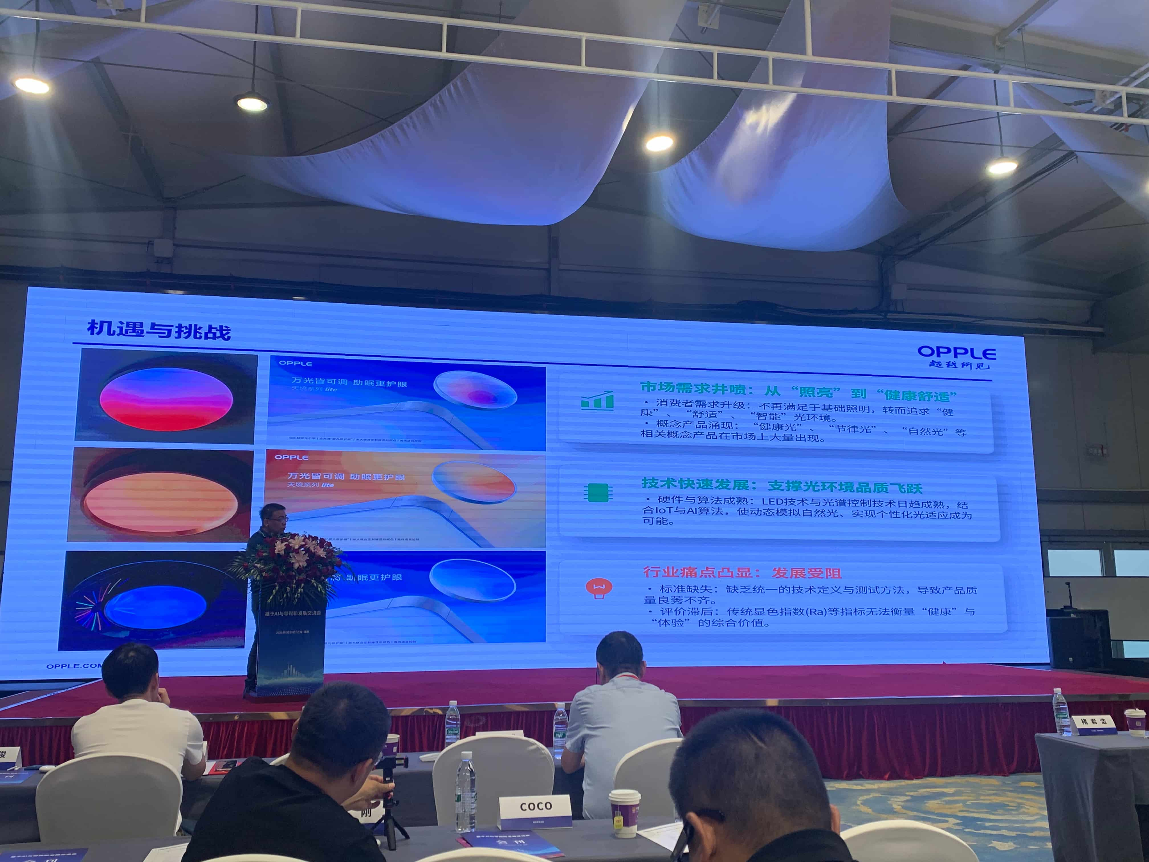
    Last week, I attended the 2026 SILA Member Annual Conference & *New Development Exchange Based on AI and Net-Zero*. Thirteen sessions in one day—twelve presentations plus a roundtable discussion—packed with insights.

    After the event, I found myself asking: If I had to sum up the signal from this conference in one sentence, what would it be?

    Not “AI is hot,” and not “dual carbon is important”—those are true but unhelpful truisms. What really matters is that several things have shifted from “optional” to “mandatory,” and the industry is quietly reaching a turning point.

    Today, let me walk you through three definitive inflection points I see.

    ## 1. Matter: From Optional to Mandatory

    Matter was the first topic raised at the conference and a key priority for SILA. Lighting manufacturer OM’s strategy is to act as the **certification principal** and license the certification to its clients.

    The signal is clear: for lighting product exporters, Matter is no longer a question of *whether* to do it, but a question of *when* you’ll finish it.

    Why? Because pressure is trickling down from overseas channels and platforms. Leading consumer brands like Philips Hue, Govee, and Nanoleaf completed Matter integration long ago. If smaller brands can’t keep up, their competitiveness on platforms like Amazon will fall sharply.

    More importantly, Matter isn’t just a protocol—it demands a full stack of software capabilities: device onboarding, local control, cross-ecosystem interoperability. Hardware-only factories without software development capabilities won’t even clear the Matter threshold.

    Which brings me to the second inflection point.

    ## 2. Software Capability: From Bonus Feature to Competitive Divide

    One observation really stood out at this conference: LED chip manufacturers are no longer just talking about chip specs.

    What are they doing instead? They’re packaging “chip + optics + dimming algorithms” into complete solutions and empowering finished-goods manufacturers.

    This is completely different from five years ago. Back then, chip makers competed on hard parameters—efficacy, CRI, lifespan. You’d pull up a datasheet and the customer would pick. Not anymore. What customers want isn’t just a chip—it’s a complete answer: *How does this chip work in my product? How do I dim it? How do I connect it?*

    Moving up the value chain, the divergence at the brand level is even starker.

    Major consumer brands (Hue, Govee, Nanoleaf, etc.) have in-house R&D—they build their own apps, voice control, and scene automation. Smaller players without those capabilities rely on third-party platforms like Tuya or Xiaomi Home.

    And what about the manufacturers in between? They used to compete on hardware manufacturing capacity—whoever had the biggest output and the lowest cost won. That capability is now becoming an industry baseline. What really separates winners from losers is **software development service capability**: can you customize lighting profiles for different user segments, tune dimming curves for specific scenarios, build custom app interfaces on demand…

    Hardware is the foundation. Software is the future divide.

    ## 3. EU Carbon Regulations: From Distant Concern to Immediate Pressure

    If the first two inflection points are technical, the third is regulatory—and more urgent.

    The conference discussion of EU carbon taxes, carbon footprint, and packaging regulations was no accident. Several of these rules are already taking effect.

    – **PPWR (Packaging and Packaging Waste Regulation)** — fully implemented as of August 12, 2026. Lighting packaging exported to Europe—cartons, foam cushioning, stretch wrap, pallets—is all subject. Companies need to complete EPR registration and declarations of conformity *immediately*. Not “soon.” *Now.*
    – **CBAM (Carbon Border Adjustment Mechanism)** — currently covers steel and aluminum, but aluminum housings and aluminum PCBs in LED fixtures are downstream products. When CBAM expands in 2028, they’ll likely be directly impacted.
    – **ESPR + DPP (Carbon Footprint Regulations)** — ICT and electronics are expected to fall under delegated acts between 2027 and 2028. At that point, carbon footprint declarations and Digital Product Passports will become market access requirements.

    Taken together, the message is clear: lighting companies serving the European market need to start building Product Carbon Footprint (PCF) data systems now. In two or three years, they might not even clear the entry bar.

    And this isn’t just for exporters. China’s own “dual carbon” policies are advancing too. The Shanghai Energy Efficiency Center’s presentation specifically covered 15th Five-Year Plan dual-carbon policies and industrial development. Companies shifting from export to domestic sales, and those serving domestic engineering projects, will face carbon footprint requirements sooner or later.

    > Prepare early, stay ahead.

    ## Final Thoughts

    These three inflection points are essentially three sides of the same coin: **the lighting industry is shifting from “selling hardware” to “selling solutions + services.”**

    – Matter is standardization at the protocol level
    – Software capability is differentiation at the product level
    – Carbon regulations are threshold-setting at the compliance level

    For companies, this isn’t a question of *whether* to transform—it’s a question of *how fast* you can do it. Winners of the hardware era won’t necessarily keep winning in the software era. Chip makers competing only on specs may be outpaced by competitors offering complete solutions. OEM factories may find themselves locked out by both Matter and carbon footprint requirements.

    The turning point is here. Are you ready?

    —

    *Version 1.0 | Written by LED Product Manager | August 25, 2026 | Dongguan*